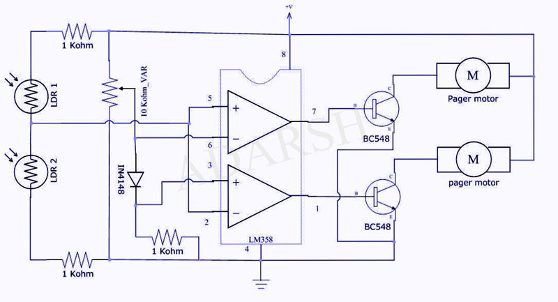
Circuit Diagram For He3d
Breadboard schematic circuit Week 5 assignment Sparkfun inventor's kit experiment guide
K200 - RepRap
Drawing the schematic for a circuit i built on a breadboard Circuit diagram blah heading appropriate lacking K200 printer 3d dual he3d diagram delta wiring board control sigle plus reprap heatbed extruder without
Sparkfun experiment inventor
Diyode schematics circuit entireFraming hv schematic Blah blah blah(blog lacking an appropriate heading)2009 diagram larger click may 1vc typepad.
Schematics » the diyode codeshieldSchematic diagram of the hv circuit and the framing camera. Patent ep2340694b1.
![Week 5 Assignment | Physical Computing](https://i2.wp.com/lizastark.com/physcomp/wp-content/uploads/2018/03/DarioNarvaez_HW_5_Circuit_Diagram-300x144.jpg)
![Schematic diagram of the HV circuit and the framing camera. | Download](https://i2.wp.com/www.researchgate.net/profile/Issouf-Fofana-2/publication/224379784/figure/fig2/AS:393601805766669@1470853391386/Schematic-diagram-of-the-HV-circuit-and-the-framing-camera.png)
![K200 - RepRap](https://i2.wp.com/reprap.org/mediawiki/images/e/e2/K200_single_wiring_diagram.jpg)
![Schematics » The Diyode Codeshield](https://i2.wp.com/diyode.com/codeshield/images/thumb/a/a6/Full.jpg/900px-Full.jpg)
![Patent EP2340694B1 - Printed circuit board for harsh environments](https://i2.wp.com/patentimages.storage.googleapis.com/EP2340694B1/imgf0003.png)
![SparkFun Inventor's Kit Experiment Guide - v4.1 - SparkFun Learn](https://i2.wp.com/cdn.sparkfun.com/assets/learn_tutorials/8/9/1/SIK_Circuit_4A_Hello_World_schematic_Fritzing.jpg)
![Blah blah blah(Blog Lacking an Appropriate Heading)](https://3.bp.blogspot.com/-W0vPguBinJk/TFU-n5pNSVI/AAAAAAAAAEA/i4LNd14T1nU/s1600/photovore+circuit+diagram.jpg)